Tech Talk
Understanding NAND Flash Technology
Last updated 7 May 2024
What is NAND Flash?
NAND Flash is a type of non-volatile storage technology that does not require power to retain data. An everyday example would be a mobile phone, with the NAND Flash (or the memory chip as it’s sometimes called) being where data files such as photos, videos and music are stored on a microSD card. NAND flash chips are roughly the size of a fingernail and can retain huge amounts of data.
Where is it used?
NAND is primarily found in memory cards, USB flash drives, and solid-state drives. NAND Flash is all around us – in our smartphones, modern televisions and in the computers and tablets in our homes and offices. It is also found outside, in all sorts of equipment from traffic lights to digital advertising panels, passenger announcement systems and displays. Anything that has artificial intelligence (AI) and needs to transfer and retain data is likely to contain NAND Flash.
NAND Flash is available in different grades; industrial and consumer. There are significant differences between industrial and consumer-grade NAND, so it is important to consider the impacts these differences have on reliability, endurance, compliance and total cost of ownership (TCO) before selecting the NAND Flash that is fit for purpose in your application.
Why is it used?
Devices made using NAND Flash offer mechanical shock resistance, and high durability and are able to withstand high pressure and temperature when compared to traditional hard disk drives. There are no moving parts, unlike HDDs, so are ideal for systems that vibrate and shake. NAND also offers fast read access times which is crucial when processing lots of data.
What are its limitations?
NAND has a finite number of read/write cycles in a specific block (each time a bit is written or erased constitutes a program/erase cycle). Once a device reaches the user and is in operation (following manufacturer early life failure tests) its first day is always its best. NAND failure is inevitable once the program erase cycles limit is reached. Individual cells fail and overall performance degrades, a concept known as wear-out.
Why is wear-out important?
When the NAND fails the device becomes unusable, resulting in the loss of data and application functionality.
How can I prevent this from happening?
The simple answer is you can’t! Advanced wear-leveling, overprovisioning and firmware algorithms, can all help to increase NAND endurance. However, the best method is to understand your data usage and what the limitations are of each type of NAND used. Together with endurance technology you can protect your applications functionality and data.
How is NAND made?
The way that NAND Flash is made can have a dramatic outcome on the performance characteristics.
NAND Flash goes through over 800 different manufacturing processes and it takes around 30 days to make just one wafer which is the size of a large pizza, typically 300mm in diameter. NAND factories or ‘FABS’ are huge, run 24/7, 365 days a year for maximum efficiency and are 100 times cleaner than hospital operating theatres. FABS can make different types of NAND Flash (SLC, MLC, 3D LTC – more on that below) and come in different sizes. Some of the largest FABS can make over 100,000 wafers a month.
Once the wafer is divided, or cut into separate chips, these are analysed and graded as 1,2,3 or 4, with 1 being the highest quality. The chips are then shipped to a vendor, such as Kingston Technology, who uses the NAND in their own products. The highest quality chips will have the best performance characteristics and therefore a price premium.
Key NAND characteristics – side by side
| SLC | 3D TLC | pSLC | Industrial MLC | TLC | |
| Reliability | Highest | High | High | Medium | Low |
| Speed | Fastest | Fast | Fast | Medium | Slow |
| Price | ££££ | £ | £££ | ££ | £ |
| P/E Cycles/Endurance | ***** | ** | **** | *** | ** |
| Warranty | 5 years | 2-5 years | 2-5 years | 2 years | 2years |
| Operating Temp -40°C to 85°C | Yes | Yes | Yes | Yes | No |
| Operating Temp 0°C to 70°C | Yes | Yes | Yes | Yes | Yes |
| Controlled BOM | Yes | Yes | Yes | Yes | No |
| Typical NAND Production Cycle | 5 years | 1-2 years | 3 years | 3 years | 6-12 months |
Differences between NAND Flash types
There are pros and cons for each type of NAND Flash. SLC holds less data but is very fast and has the highest endurance. It is however the most expensive. Other types of NAND can hold more data and are cheaper but have much lower endurance levels and are often slower. So, when deciding which NAND flash is suitable for an application it is important to carefully consider these characteristics and their impact on application performance. If you are not sure, seek specialist advice.
Probably the key differentiator between NAND types is the endurance or Programme Erase (P/E) cycles. Due to the way NAND Flash memory works, it is required that a cell is erased before it can be written to. The process of erasing and then writing a cell is called a P/E cycle. Each time a cell is erased it is damaged or worn out, so there is a lifetime for each cell. This is exacerbated by the makeup of NAND Flash. A cell can only be erased as a block and is written as a page. The size of each block and page is dictated by the design of the NAND Flash chip, but a block consists of many pages. If the information in a cell change, it is written to a different cell and the old data is marked as ‘ready for deletion’. Then, the ‘good’ data in a block is moved elsewhere and the whole block is erased.
So, often even if data in a cell does not change it will still go through a P/E cycle. Cells are worn as equally as possible using wear-levelling technology. This whole process increases the number of P/E cycles and ensures that the NAND Flash does not fill up with redundant data. The lifetime of the device is defined as endurance and is proportional to the P/E cycles of the NAND Flash. Remember earlier about storing bits of data in each cell?
In comparing the different types of NAND the typical P/E cycles are as follows:
- SLC 60,000
- MLC 1,500 to 3,000 (lower endurance for consumer/higher for industrial)
- 3D TLC 500 to 3,000 (lower endurance for consumer/higher for industrial)
As can be seen, there is a considerable difference in NAND endurance and selecting the wrong type will have an impact on application performance and could ultimately shut down your system. Get the right type of NAND in your system by speaking to Simms. Buy once, buy right.
Depending on device and Flash configuration, SLC can have even higher programme erase cycles, with some tests reported to be in excess of 100,000 which is a phenomenal amount.
Bridging the Gap with pLSC (SLC mode)
SLC mode is a hybrid of 2-bit per cell MLC or 3D TLC Flash using intelligent firmware to emulate the storage states of SLC. This results in increased endurance of around 20-30K P/E cycles (althogough potentially this could be much higher depending on device and Flash configuration) at only a fraction of the cost when compared to SLC. For industrial applications where cost and reliability are of equal importance, this offers a good middle ground. In the marketplace, SLC mode is often referred to as pSLC and some manufacturers have their own brand names, such as iSLC and aMLC, but essentially these are all the same thing.
Which NAND type is right for my application?
Each application will have different demands on endurance, temperature, performance and data retention so it will depend on which criteria are most important. Generally, for industrial applications where quality, reliability and longevity of supply are required, SLC, pSLC or industrial grade level MLC is used. For consumer-based technology, where the impact of losing functionality or data is not severe and devices are typically thrown away or replaced at low cost, TLC or 3D TLC will be used.
What is 3D NAND?
3D NAND is now the major player in the NAND Flash market. Although the concept of 3D NAND is not new (it has been around for almost a decade) it has only made its way into the market in a big way in the last couple of years. It is arguably the biggest NAND development since its inception in the 1980s but getting 3D NAND to work consistently has been an issue. However, these challenges have now been overcome and 3D NAND will doubtless be the NAND Flash of choice for years to come.
In layman’s terms, 3D NAND is the stacking of memory chips on top of each other. Some manufacturers call this V (for vertical) NAND. The aim of this NAND is to make applications and devices run faster and more efficiently, hold more information and use less energy. The first company to launch 3D NAND was Samsung, a household name and by far the world’s largest NAND Flash manufacturer, with over 40% of the global NAND market.
Getting 3D NAND to work consistently in wide operating temperatures (-40°C to 85°C) has been a challenge for some manufacturers who supply the industrial markets. The standard operating temperature of 0°C to 70°C is adequate for consumer-grade, workplace, server and data centres but for applications working in harsh environments or remote places this temperature range is not enough. Industrial storage providers have now had time to analyse and test 3D NAND to the point where it consistently works in wide operating temperatures and it is now available for industrial applications.
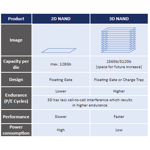
3D NAND flash offers higher capacity in a smaller physical space than 2D NAND. In comparison to planar NAND, 3D NAND can lower the cost per gigabyte, may improve electrical use to reduce power consumption, boost reliability, and provide higher data write performance.
Should I use 3D NAND for my application?
This is a question we get asked all the time but it really depends on what you are using the storage in your application for. 3D NAND may be suitable but it’s always worth speaking to experts to get the right solution.
Questions?
There is a fair deal to understand regarding NAND flash and we have barely scratched the surface with our overview (We don’t want to get too technical as that will only confuse matters). So if you are using SD cards microSD, SSD, USB, mSATA, M.2 or any other form factor in which you are experiencing issues, then why not get in touch we will be delighted to assist you. Our technical experts are ready and waiting.