Tech Talk
3D NAND: An Introduction and Overview
Last updated 12 July 2022
Here at Simms, we like to keep our customers and visitors to our website informed of developments in memory and storage. Arguably, one of the biggest, if not the most significant developments in the last 30 years is the introduction of 3D NAND Flash. The concept of 3D NAND is familiar; it has been around for several years, but getting it working consistently has been a challenge.
What is 3D NAND?
In simple terms, 3D NAND is stacking memory (or silicon) chips on each other. Some manufacturers call this V (for vertical) NAND. The aim is to make your device faster, hold more information, run more efficiently and use less energy.
The concept has been around for several years, but developments have only taken a significant step forward. The first to launch was Samsung, a household name that is by far the largest NAND Flash manufacturer, with 40% of the global market. Other manufacturers are now following suit. This switch led to shortages in 2017 for 2D NAND (which is still extremely popular.)
NAND Flash Shortages - a guide from Simms on Vimeo.
How is 3D NAND made?
2D NAND Flash goes through over 800 processes to make just one wafer (the size of a large pizza). One wafer takes around 30 days to make and then shipped to a vendor, such as Kingston, who adds the NAND to their products.
NAND Factories or ‘FABS’ are huge, run 24/7, 365 days for maximum efficiency, and are 100 times cleaner than hospital operating theatres. 3D NAND requires even more processes as the cells are stacked on top of each other.
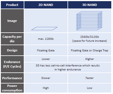
3D NAND is more difficult to make than previously thought, and unlike 2D NAND, which is a planar structure, 3D NAND resembles a vertical skyscraper. A 3D NAND device consists of multiple levels or layers stacked and then connected using tiny vertical channels.
Today’s leading-edge 3D NAND parts are 32- and 48-layer devices. Scaling 3D NAND to 64 layers and beyond presents significant challenges, but some manufacturers already target 96 layers. 3D NAND is expected to hit the ceiling at or near 112 layers in future.
Beyond 3D NAND
To extend 3D NAND beyond 128 layers, the industry is quietly developing a technology called string stacking. Still, in R&D, string stacking involves stacking individual 3D NAND devices on top of each other. For example, if one stacks three 64-layer 3D NAND devices on top of each other, the resulting chip will represent a 192-layer product.
The trick is to link the individual 64-layer devices with some interconnecting scheme. This is a complex technology to develop. According to experts, even with string stacking, 3D NAND would top out at or around 300 layers.
To learn more, click the video (below) to watch how Toshiba (the second-largest NAND manufacturer) manufactures 2D NAND Flash.
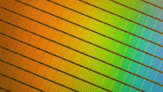
The image illustrates how current 2D and 3D NAND compare in their structure. Although 3D NAND is slower than RAM, it certainly bridges the gap between current NAND and RAM.
Where are we now?
3D NAND is readily available in mainstream consumer devices like smartphones, tablets, and computers. Intel uses 3D NAND across their entire range of SSDs, including data centres and personal and enthusiast data storage.
On the industrial side, 3D TLC is very much in mainstream industrial form factors such as 2.5", mSATA, M.2 and slimSATA, with capacities already hitting 1TB and sometimes 2TB.
As manufacturers continue to explore and push the boundaries of 3D NAND, we can, in the future, expect to see larger capacities and quicker speeds.
Future of SLC, pSLC and MLC
3D NAND is a considerable development and undoubtedly has its plus points. But is it ideal for industrial applications? Like most things, it depends on what you are using it for. 3D industrial is a high capacity and lower cost NAND than SLC and MLC flash. SLC AND MLC are not going anywhere overnight; supply and demand are still strong for both, given their performance characteristics. However, we have recently published an article on the future of MLC NAND, which explains the changes in the market during COVID. Please read it here.
3D NAND is well worth a look alongside SLC and MLC products and sits at the lower end of the pricing scale. We know this technology, and expert help is at hand to ensure you get the right-first-time solution.